Semiconductor
Semiconductor Seals and Services
M Barnwell Services offers an extensive range of Semiconductor Seals designed to excel in deposition, etch, ash/strip, plasma, wet chemical, and thermal processes. These versatile products cater to various sectors within the semiconductor and related manufacturing industries, including:
- Logic and memory.
- MEMS.
- HBLED.
- Power Devices.
- Solar cells (crystalline, multi-crystalline, concentrator).
- Flat panel display (LED / OLED).
- Optoelectronics.
Choose reliability and performance across diverse applications with our comprehensive Semiconductor Seals range.
Types of Seals
Semiconductor O Rings
O Rings play a critical role in maintaining the integrity of various processes within the semiconductor industry. These seals are designed to provide reliable and consistent performance in environments where precision, cleanliness, and chemical resistance are paramount. Here’s more extensive information about Semiconductor O Rings:
Materials: Semiconductor O Rings commonly withstand the demanding conditions of semiconductor manufacturing processes using high-performance materials. We choose materials such as Perfluoroelastomers (FFKM), Fluorocarbon (FKM or Viton™), and other specialty elastomers for their exceptional chemical resistance, thermal stability, and low outgassing properties.
Chemical Resistance: Semiconductor processes involve exposure to a variety of chemicals, including aggressive acids, bases, and solvents. O Rings for the semiconductor industry are formulated to resist chemical degradation and maintain their sealing integrity over extended periods.
Temperature Resistance: Semiconductor manufacturing often involves extreme temperature variations. O Rings used in this industry are engineered to withstand both low-temperature and high-temperature conditions. This ensures consistent performance across a broad temperature range.
Cleanroom Compatibility: Semiconductor manufacturing facilities operate in cleanroom environments to prevent contamination. Produced and packaged with meticulous care, O Rings minimise particle generation to ensure compatibility with stringent cleanroom standards. Our Clean Room Facility ensures we uphold that expectation.
Fully moulded Imperial and Metric O Rings can be manufactured from micro-miniature and to any quantity. Custom non-standard sizes are also available.
Centering Rings / Flange Fittings
Centering rings made from aluminum or stainless steel can be seamlessly paired with any elastomer material offered by M Barnwell Services. These versatile centering rings are accessible in a range of sizes. They conform to standards such as NW, KF, and ISO, providing flexibility and compatibility for diverse applications.
Slit Valve Doors
We offer a diverse selection of materials and profiles. All of these are designed to enhance sealing integrity and the overall lifespan of slit valve doors, whether bonded or non-bonded, as well as MONOVAT® gates.
Our comprehensive range ensures that you can choose the ideal combination of materials and profiles tailored to meet your specific requirements. Count on us to provide solutions that optimise performance and durability for these critical components in your applications.
Special Rubber Mouldings and Extrusions
We expertly design and craft our seals to meet your specific requirements, tailoring them precisely to your needs. These seals possess the capability to be molded into a wide array of shapes, sizes, and profiles, providing virtually limitless possibilities for customisation.
Explore further details on our Special Rubber Mouldings and Extrusions by clicking here. Your specific semiconductor sealing needs are our priority, and we provide versatile solutions to ensure optimal performance in your applications.
Lip Seals
Lip seals offer an effective solution for sealing wider gaps that demand substantial deflection, particularly in scenarios where there is a constraint on available contact force. This versatile sealing option ensures reliable performance in situations where creating a secure seal with limited contact force is essential. Choose lip seals for their ability to provide efficient sealing in challenging conditions, adapting to the specific requirements of applications with wider gaps and deflection challenges.
End-effector Pads / Wafer Handling Components
Designed to provide solutions for wafer handling applications, end effector pads deliver low contact force and electrostatic dissipative properties. Our extensive range of materials provides options with varying coefficients of friction, allowing the customisation of wafer retention force according to specific needs. Additionally, we offer the flexibility of creating custom designs for end effector pads, ensuring a tailored approach to meet the unique requirements of your wafer handling processes.
In collaboration with industry leaders, we engage in an ongoing development program that ensures the continuous evolution of elastomers. Our commitment is not only to meet the current demands of the industry but also to anticipate and address future requirements.
Utilising M Barnwell Services Semiconductor elastomer materials offers several advantages, including:
- Extended Tool Preventative Maintenance (PM) Cycles:
Our elastomers contribute to extended PM cycles for tools, enhancing their operational longevity and reducing the frequency of maintenance. - Reduced Process Defects:
The use of our elastomer materials helps in minimising process defects, ensuring a smoother and more reliable semiconductor manufacturing process. - Lower Particle Generation:
M Barnwell Services Semiconductor elastomers are designed to minimise particle generation, supporting the maintenance of a cleaner and contamination-controlled environment. - Increased Tool Efficiency:
The inherent properties of our elastomers contribute to increased tool efficiency, optimising the overall performance of semiconductor manufacturing tools. - Reduced Cost of Ownership:
With the benefits of extended maintenance cycles, lower process defects, and increased tool efficiency, our elastomer materials contribute to a reduced cost of ownership over the lifespan of semiconductor tools.
Extreme Seals

When specific temperatures necessitate exceptional wear resistance, we offer an industry-leading selection of Extreme Seals. Our comprehensive range is designed to excel in demanding conditions, providing optimal performance and durability where wear is a critical factor.
Garlock Speciality Semiconductor Seals
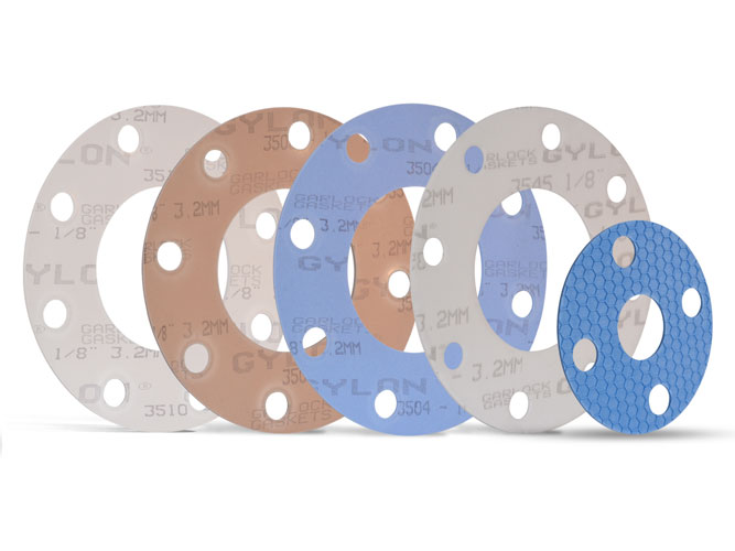
Garlock’s STRESS SAVER® 3522 technology is a cutting-edge solution utilising 100% pure and restructured PTFE. This innovative approach ensures exceptional chemical compatibility with various substances, minimal leachable contaminants, and easily cleanable contact surfaces, actively discouraging the growth of bacteria. Engineered with efficiency as a priority, the STRESS SAVER® 3522 is versatile, and suitable for both high-stress raised face flanges and low-stress non-metallic flange designs. This versatility streamlines the selection process and guarantees long-term dependability.
The GYLON® Style 3545, featuring microcellular PTFE, stands out with exceptional compressibility, further enhanced by a rigid PTFE core for improved manageability. Purpose-built for its remarkable ability to compress and conform to irregular or damaged surfaces, the GYLON® 3545 excels in applications where flanges generate lower compressive stresses. This makes it the ideal choice for scenarios involving glass-lined flanges and equipment.
For a deeper dive into the features and benefits of both of these seals, visit our Semiconductor Manufacturing Seals page.
Inflatable Seals
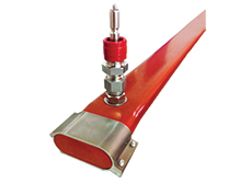
An Inflatable Seal, a flexible rubber seal designed to expand and contract in response to an inflation source, offers versatility by maintaining its original shape upon deflation. Functioning axially, radially inward, or outward, these seals typically use regulated air as the inflation medium, with specific applications potentially requiring liquid for inflation.
In the Semiconductor industry, Inflatable Seals prove highly effective for load lock seals, thermal processing, and circuit board imaging, particularly excelling in sealing non-standard gaps where fixed seals may encounter challenges.
Our services extend beyond information provision; we offer on-site consultation, sample identification, and technical support tailored to your requirements. Explore the range of Semiconductor Material Grades here, and gain insights into Plasma, Thermal, and Wet Processes on the Semiconductor Manufacturing Process page.
Contact us for comprehensive details on solutions we can offer you, or request a quote. Your semiconductor sealing needs are our priority, and we are here to provide tailored solutions and support throughout the process.
E&OE

